Scanning Probe Microscopy
Radboud University, Nijmegen
Research
Our group approaches numerous problems in physics and chemistry, utilizing or innovating new state-of-the-art methods in scanning probe microscopy (SPM). Our aim is to understand fundamental problems ultimately toward innovating new approaches to technological applications based on materials science. Our expertise focuses on high precision structural, electronic and magnetic imaging in cryogenic ultrahigh vacuum environments and in magnetic fields.
To warrant the highest quality of our samples, we prepare them ourselves in situ, i.e., within the ultrahigh vacuum (UHV) systems to which the cryogenic SPMs are connected. Sample preparations involve cleaning of single crystal surfaces (cleaving, sputtering, annealing,...), often followed by molecular beam epitaxy (MBE) and/or chemical vapor deposition (CVD) to deposit ultrathin films or sub-monolayer amounts of adsorbates. Low-temperature deposition is often used to adsorb individual atoms and molecules on our surfaces. This is usually combined with SPM-based atomic manipulation of these adsorbates.
Below, you can find a selection of research topics and projects conducted in our group. We also offer more information on the SPM methodology used in our group as well as an overview of our instrumentation and their main specifications. Finally, our SPM image gallery shows some beautiful examples.
Topics
Complex magnetism on surfaces
We are interested in surface magnetism beyond the collinear limit, and how interface-driven interactions can lead to new complex magnetic phases of matter, for example skyrmionic or chiral spin order. To this end, we employ spin-polarized scanning tunneling micropscopy (SP-STM) and magnetic exchge force microscopy (MExFM), which in combination we refer to as SPEX.
We are interested in surface magnetism beyond the collinear limit, and how interface-driven interactions can lead to new complex magnetic phases of matter, for example skyrmionic or chiral spin order. To this end, we employ spin-polarized scanning tunneling micropscopy (SP-STM) and magnetic exchge force microscopy (MExFM), which in combination we refer to as SPEX.
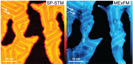 Spin spiral network in 2 ML Fe/Ir(111) [1].
 A few years ago, we also discovered the unprecedented complexity of bulk neodymium, a rare-earth metal, which surprisingly has a glassy magnetic ground state. Since then, we have been continuedly studying this material, in order to unravel the behavior of this new type of spin glass.
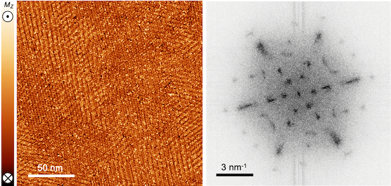
Magnetizaton image and 2D FFT of the spin-glass state of bulk-like Nd(0001) films on W(110) [2].
Artificial quantum matter – atom by atom
We utilize surfaces combined with patterned atomic impurities as a platform to create electronic and magnetic artificial lattices. For example, with this method, we can utilize these platforms as a testbed to realize new states of matter. This on-surface quantum simulator allows for testing many cutting-edge theories about the electronic and magnetic behavior of matter in one and two dimensions.
We utilize surfaces combined with patterned atomic impurities as a platform to create electronic and magnetic artificial lattices. For example, with this method, we can utilize these platforms as a testbed to realize new states of matter. This on-surface quantum simulator allows for testing many cutting-edge theories about the electronic and magnetic behavior of matter in one and two dimensions.
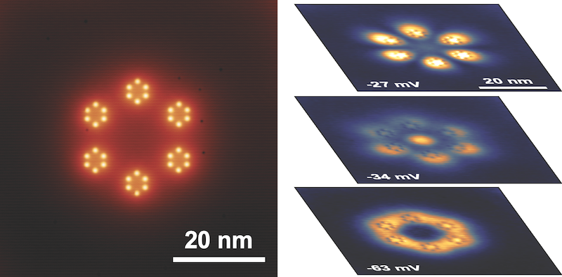 Topography (left) and sequence of orbital images of artificial benzene, created by manipulating 36 Cs atoms on the InSb(110) surface [3].
Van der Waals Materials
We want to understand exotic electronic and magnetic phases in van der Waals materials, and the role of atomic-scale defects or impurities. Moreover, we are interested in how dimensionality alters the properties of van der Waals materials when approaching the single-layer limit (referred to as 2D materials), and the changes to electronic screening in these environments.
We want to understand exotic electronic and magnetic phases in van der Waals materials, and the role of atomic-scale defects or impurities. Moreover, we are interested in how dimensionality alters the properties of van der Waals materials when approaching the single-layer limit (referred to as 2D materials), and the changes to electronic screening in these environments.
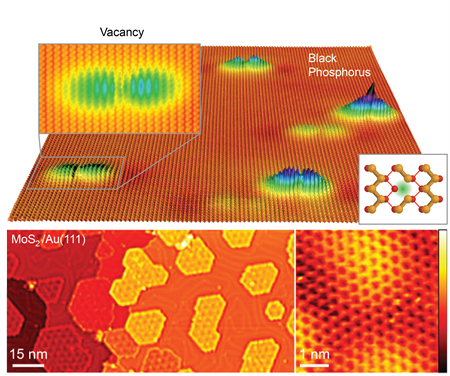
Top: Defects on the surface of black phosphorus [4]. Bottom: Single-layer MoS2/Au(111) [5].
Neuromorophic materials and brain-inspired computing
We are interested in utilizing the control we have of individual atomic (spin) states as well as coupling between atoms and atomic spins, as a platform to investigate various types of brain-inspired computing concepts [6,7].
We are interested in utilizing the control we have of individual atomic (spin) states as well as coupling between atoms and atomic spins, as a platform to investigate various types of brain-inspired computing concepts [6,7].
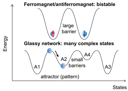
Schematic of the energy landscape differences between bistable memory, and the energy landscapes of interest for brain-inspired hardware.
Single-molecule light emission
We perform submolecularly resolved fluorescence studies by combining STM with detection of light emitted from the tunnel junction. This allows for novel fundamental studies of opto-electronic properties and light-matter interactions, e.g. exciton formation and decay [8], plasmon-exciton coupling [9] or resonant energy transfer [10].
We perform submolecularly resolved fluorescence studies by combining STM with detection of light emitted from the tunnel junction. This allows for novel fundamental studies of opto-electronic properties and light-matter interactions, e.g. exciton formation and decay [8], plasmon-exciton coupling [9] or resonant energy transfer [10].
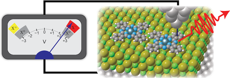
Schematic of the voltage-dependent single-molecule fluorescence of a ZnPc molecue in an STM junction [8].
Superconductivity in ultrathin films
Superconductivity in ultrathin films
We study the properties of superconductors in the ultathin film limit, which can lead to a significant increase of the critical temperature and in-plane critical field [11]. Moreover, interface effects can become relevant [12]. Ultrahin superconductors can be used to study their interaction with single atomic or moleclar adsorbates in magnetic fields.
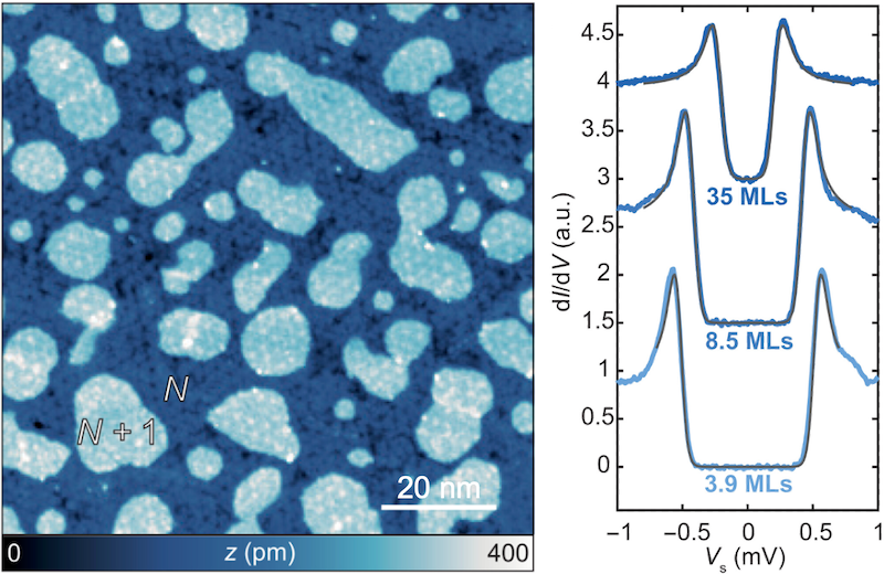
Ultrathin films of Al/Si(111) show an up to threefold enhancement of superconductivity [11].
References
- N. Hauptmann, M. Dupé, T.-C. Hung, A. K. Lemmens, D. Wegner, B. Dupé, A. A. Khajetoorians, Revealing the correlation between real-space structure and chiral magnetic order at the atomic scale, Physical Review B 97, 100401 (2018).
- U. Kamber, A. Bergman, A. Eich, D. Iuşan, M. Steinbrecher, N. Hauptmann, L. Nordström, M. I. Katsnelson, D. Wegner, O. Eriksson, A. A. Khajetoorians,Self-induced spin glass state in elemental and crystalline neodymium, Science 368, eaay6757 (2020).
- E. Sierda, D. Badrtdinov, B. Kiraly, E. Knol, X. Huang, M. I. Katsnelson, G. C. Groenenboom, D. Wegner, M. Rösner and A. A. Khajetoorians, Quantum simulator to emulate lower-dimensional molecular structure, Science 380, 1048 (2023).
- B. Kiraly, N. Hauptmann, A. N. Rudenko, M. I. Katsnelson, A. A. Khajetoorians, Probing Single Vacancies in Black Phosphorus at the Atomic Level, Nano Letters 17, 3607 (2017).
- A. Bruix, J. A. Miwa, N. Hauptmann, D. Wegner, S. Ulstrup, S. S. Gronborg, C. E. Sanders, M. Dendzik, A. G. Cabo, M. Bianchi, J. V. Lauritsen, A. A. Khajetoorians, B. Hammer, P. Hofmann, Single-layer MoS2 on Au(111): Band gap renormalization and substrate interaction. Physical Review B 93, 165422 (2016).
- A. Kolmus, M. I. Katsnelson, A. A. Khajetoorians, H. J. Kappen, Atom-by-atom construction of attractors in a tunable finite size spin array, New Journal of Physics 22, 023038 (2020).
- B. Kiraly, E. J. Knol, W. M. J. van Weerdenburg, H. J. Kappen, and A. A. Khajetoorians, An atomic Boltzmann machine capable of self-adaption, Nature Nanotechnology 16, 414 (2021).
- T.-C. Hung, R. Robles, B. Kiraly, J. H. Strik, B. A. Rutten, A. A. Khajetoorians, N. Lorente and D. Wegner, Bipolar single-molecule electroluminescence and electrofluorochromism, Physical Review Research 5, 033207 (2023).
- T.-C. Hung, B. Kiraly, J. H. Strik, A. A. Khajetoorians, D. Wegner, Plasmon-Driven Motion of an Individual Molecule, Nano Letters 21, 5006 (2021).
- T.-C. Hung, Y. Godinez Loyola, M. Steinbrecher, B. Kiraly, A. A. Khajetoorians, N. L. Doltsinis, C. A Strassert and D. Wegner, Activating the fluorescence of a Ni(II) complex by energy transfer, Journal of the American Chemical Society 146, 8858 (2024).
- W. M. J. van Weerdenburg, A. Kamlapure, E. H. Fyhn, X. Huang, N. P. E. van Mullekom, M. Steinbrecher, P. Krogstrup, J. Linder, A. A. Khajetoorians, Extreme enhancement ofs uperconductivity in epitaxial aluminum near the monolayer limit, Science Advances 9, eadf5500 (2023).
- A. Kamlapure, M. Simonato, E. Sierda, M. Steinbrecher, U. Kamber, E. J. Knol, P. Krogstrup, M. I. Katsnelson, M. Rösner, A. A. Khajetoorians, Tuning lower dimensional superconductivity with hybridization at a superconducting-semiconducting interface, Nature Communications 13, 4452 (2022).