Scanning Probe Microscopy
Radboud University, Nijmegen
Methodology
→ back to Research Overview
Scanning probe microscopes are not just microscopes to image surfaces with atomic resolution. Many additional experimental methods can be realized with SPMs, making it a versatile tool for various spectroscopies and even for bottom-up construction atomic-scale structures, Lego style. Here is a selection of techniques applied in our group.
High-resolution STM/nc-AFM
We utilize high-resolution scanning tunneling microcopy (STM) and non-contact atomic force microscopy (nc-AFM) to characterize structural and electronic properties of novel materials, including metals, novel 2D materials and thin-insulating films. We apply scanning tunneling spectroscopy (STS) with ultra-high energy resolution to explore new phases of matter, e.g. superconductivity and charge density waves.
We utilize high-resolution scanning tunneling microcopy (STM) and non-contact atomic force microscopy (nc-AFM) to characterize structural and electronic properties of novel materials, including metals, novel 2D materials and thin-insulating films. We apply scanning tunneling spectroscopy (STS) with ultra-high energy resolution to explore new phases of matter, e.g. superconductivity and charge density waves.
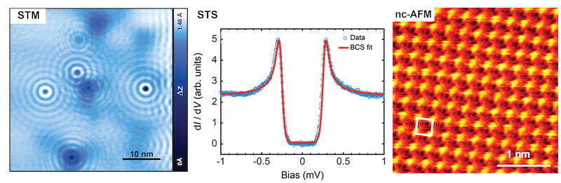
Left: Standing waves on Cu(111); middle: superconducting gap of Re(0001) [1]; right: 2 ML MgO/Ag(100) (unpublished).
Atomic manipulation
The STM can also be used to move atoms (or molecules) with atomic-scale precision. By bringing the tip very close to the atom, an attractive force between them allows for, e.g., dragging the atom along with subsequent lateral movement of the tip. In case of lateral manipulation of atoms or molecules, the tip is first lowered to the adsorbate via reduction of the tunneling resistance, and then moved laterally along the surface. This process can be repeated many times, e.g., in order to build up a nanoscale structure with a certain geometry and function, or to induce chemical reactions between different adsorbates.
The STM can also be used to move atoms (or molecules) with atomic-scale precision. By bringing the tip very close to the atom, an attractive force between them allows for, e.g., dragging the atom along with subsequent lateral movement of the tip. In case of lateral manipulation of atoms or molecules, the tip is first lowered to the adsorbate via reduction of the tunneling resistance, and then moved laterally along the surface. This process can be repeated many times, e.g., in order to build up a nanoscale structure with a certain geometry and function, or to induce chemical reactions between different adsorbates.
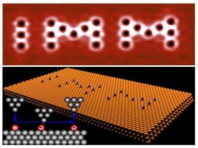
STM image (top) and 3D model (bottom) of the institute letters, assembled by manipulation of 21 CO molecules on Cu(111). The font size corresponds to 0.000006 pt (unpublished). See also [2]
Spin-resolved STM
There are two prominent methods to acquire spin information utilizing STM methods. The first is based on spin-polarized STM, in which a magnetic probe is utilized. The overall measured current has a component related to the projected magnetization of the surface onto the magnetization of the tip. Secondly, it is possible to utilize inelastic tunneling, to locally excite spin excitations, for example of individual atoms.
There are two prominent methods to acquire spin information utilizing STM methods. The first is based on spin-polarized STM, in which a magnetic probe is utilized. The overall measured current has a component related to the projected magnetization of the surface onto the magnetization of the tip. Secondly, it is possible to utilize inelastic tunneling, to locally excite spin excitations, for example of individual atoms.
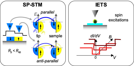
Left: Principle of SP-STM, showing the possible tunneling channels in an energy diagram. Right: Principle of inelastic tunneling, where spin-excitation threshold energies vary with external magnetic field [2].
SPEX
We have recently developed a world-wide unique combination of spin-polarized scanning tunneling microscopy and magnetic exchange force microscopy (SPEX) that can independently probe the geometric, electronics and magnetic structure and can be applied on conducting and insulating surfaces. We use SPEX for high-resolution magnetic imaging as well as for quantifying the atomic-scale magnetic exchange forces of non-collinear magnetic textures.
We have recently developed a world-wide unique combination of spin-polarized scanning tunneling microscopy and magnetic exchange force microscopy (SPEX) that can independently probe the geometric, electronics and magnetic structure and can be applied on conducting and insulating surfaces. We use SPEX for high-resolution magnetic imaging as well as for quantifying the atomic-scale magnetic exchange forces of non-collinear magnetic textures.
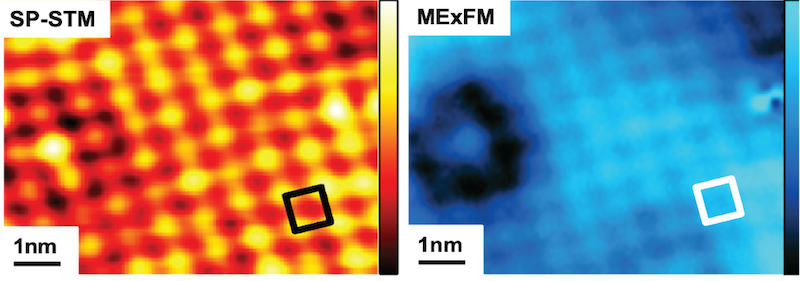
SP-STM and MExFM images of the nano-skyrmion lattice of 1ML Fe/Ir(111) [3].
STM-induced luminescence
STM-induced luminescence (STML) is based on the principle that tunneling electrons can locally excite the system (e.g. a single molecule), which can subsequently decay by emitting a photon. The light is collected in situ by a lens mounted inside the cryogenic STM, guided out of the ultrahigh vacuum system, and eventually analyzed ex situ via a grid spectrometer with an LN2-cooled CCD detector. Light intensities down to just a few photons per second can thus be detected.
STM-induced luminescence (STML) is based on the principle that tunneling electrons can locally excite the system (e.g. a single molecule), which can subsequently decay by emitting a photon. The light is collected in situ by a lens mounted inside the cryogenic STM, guided out of the ultrahigh vacuum system, and eventually analyzed ex situ via a grid spectrometer with an LN2-cooled CCD detector. Light intensities down to just a few photons per second can thus be detected.
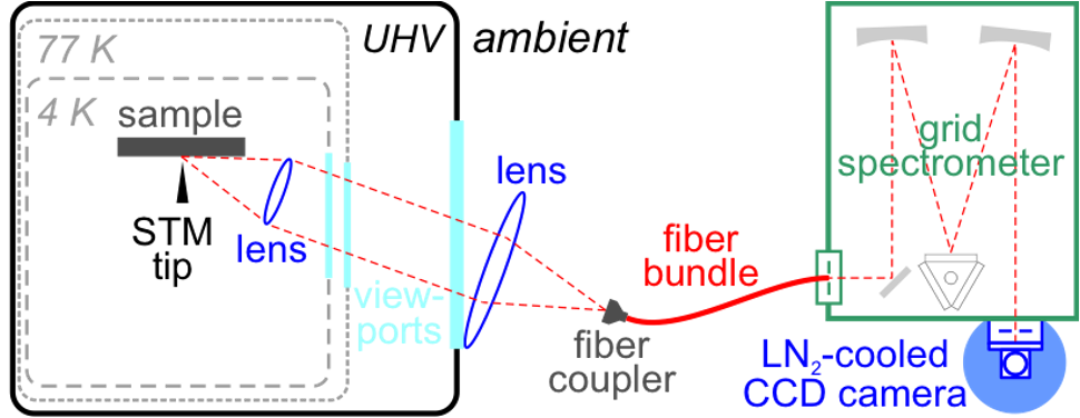
Sketch of the setup to collect and detect light emitted from a low-temperature STM junction [4].
Time-resolved STM
There are various methods to gain time-resolution in STM. Two prominent ways involve utilizing electrical excitation, via microwave waveforms. For example, pump-probe and electron spin resonance (ESR) methods can be applied to characterize the various lifetimes of individual atoms on surfaces.
There are various methods to gain time-resolution in STM. Two prominent ways involve utilizing electrical excitation, via microwave waveforms. For example, pump-probe and electron spin resonance (ESR) methods can be applied to characterize the various lifetimes of individual atoms on surfaces.
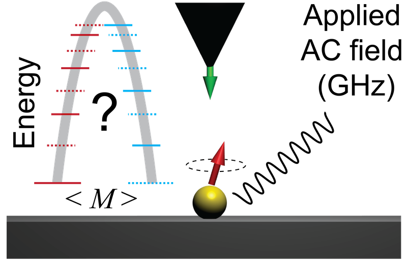
Schematic of gaining time resolution in STM, by applying GHz pulses to probe pump-probe or resonance dynamics of individual spins on surfaces [5].
References
- H. von Allwörden, A. Eich, E. J. Knol, J. Hermenau, A. Sonntag, J. W. Gerritsen, D. Wegner, A. A. Khajetoorians, Design and performance of an ultra-high vacuum spin-polarized scanning tunneling microscope operating at 30 mK and in a vector magnetic field, Review of Scientific Instruments 89, 033902 (2018).
- A. A. Khajetoorians, D. Wegner, A. F. Otte, I. Swart, Creating designer quantum states of matter atom-by-atom, Nature Reviews Physics 1, 703 (2019).
- N. Hauptmann, J. W. Gerritsen, D. Wegner, A. A. Khajetoorians, Sensing Noncollinear Magnetism at the Atomic Scale Combining Magnetic Exchange and Spin-Polarized Imaging, Nano Letters 17, 5660 (2017)
- T.-C. Hung, B. Kiraly, J. H. Strik, A. A. Khajetoorians, D. Wegner,Plasmon-Driven Motion of an Individual Molecule, Nano Letters 21, 5006 (2021).
- W. M. J. van Weerdenburg, M. Steinbrecher, N. P. E. van Mullekom, J. W. Gerritsen, H. von Allwörden, F. D. Natterer, A. A. Khajetoorians, A scanning tunneling microscope capable of electron spin resonance and pump–probe spectroscopy at mK temperature and in vector magnetic field, Review of Scientific Instruments 92, 033906 (2021).