Scanning Probe Microscopy
Radboud University, Nijmegen

SPM Image gallery
→ back to Research Overview
A side product of our research is a collection of beautiful images from the atomic world that helps to reationalize nature at the naoscale as well as quantum physics. For non-commercial use, feel free to share, but please mention our group as image course.
→ back to Research Overview
A side product of our research is a collection of beautiful images from the atomic world that helps to reationalize nature at the naoscale as well as quantum physics. For non-commercial use, feel free to share, but please mention our group as image course.
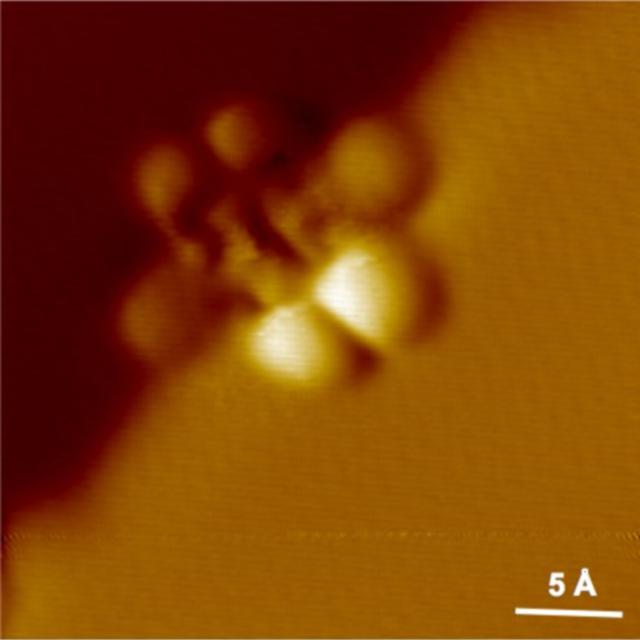 A single phthalocyanine molecule “caught” at a monatomic step edge of a Ag(111) surface, revealing a molecular orbital (LUMO). (T = 5 K)
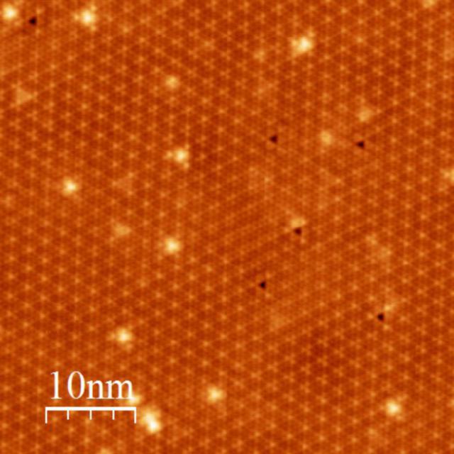 Atomic resolution of a cleaved bulk NbSe2 crystal. Superstructures correspond to the typical CDW in this material. (T = 1.2 K)
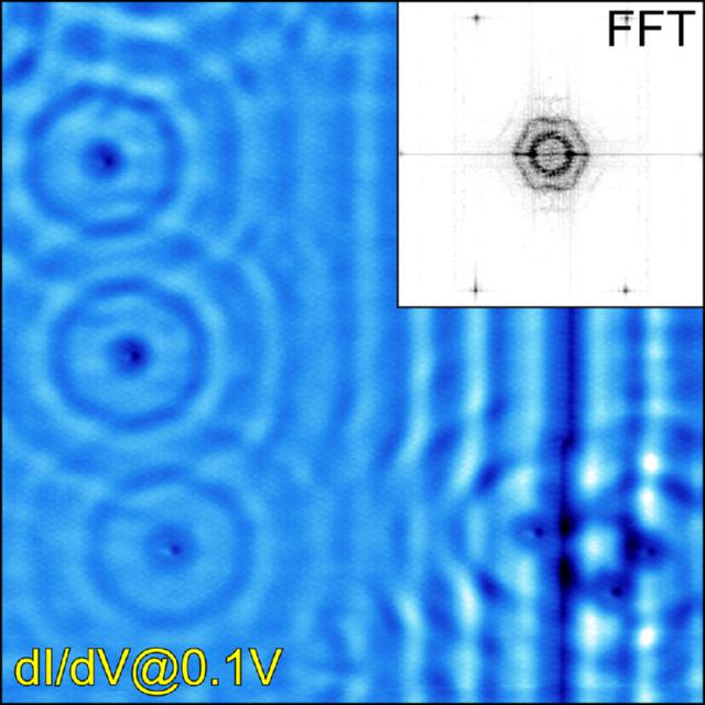
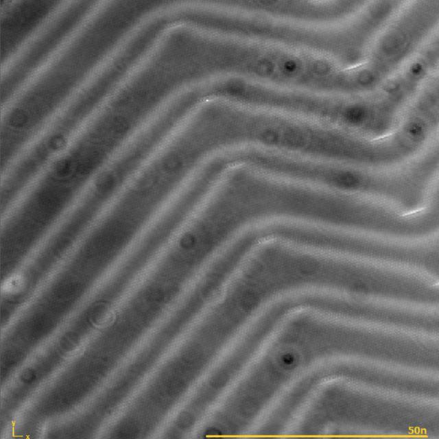 The Au(111) herringbone reconstruction with atomic resolution, and quasi-particle interference from the Shockley surface state. (T = 1.2 K)
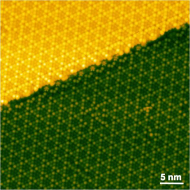 The famous Si(111)-7x7 reconstruction, the 1st atomically-resolved surface in history (Binnig & Rohrer, Nobel prize 1986). (T = 5 K)
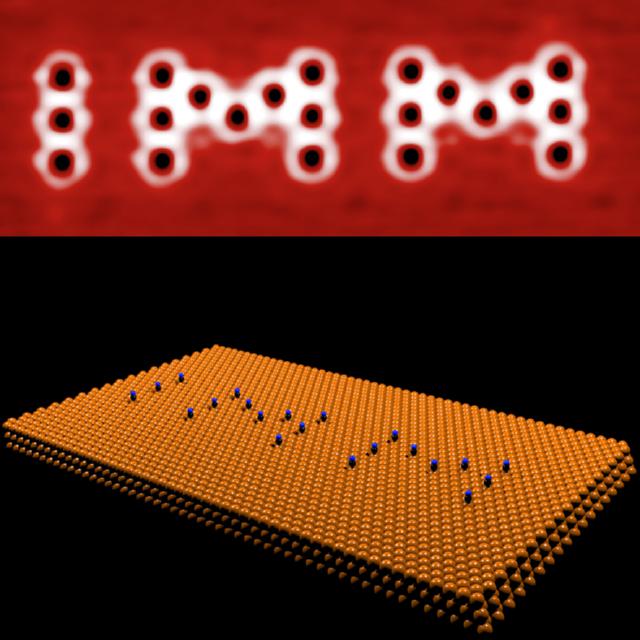 The smallest IMM logo: 21 CO molecules on Cu(111) laterally manipulated to form letters with font size 0.000006 pt. (T = 6 K)
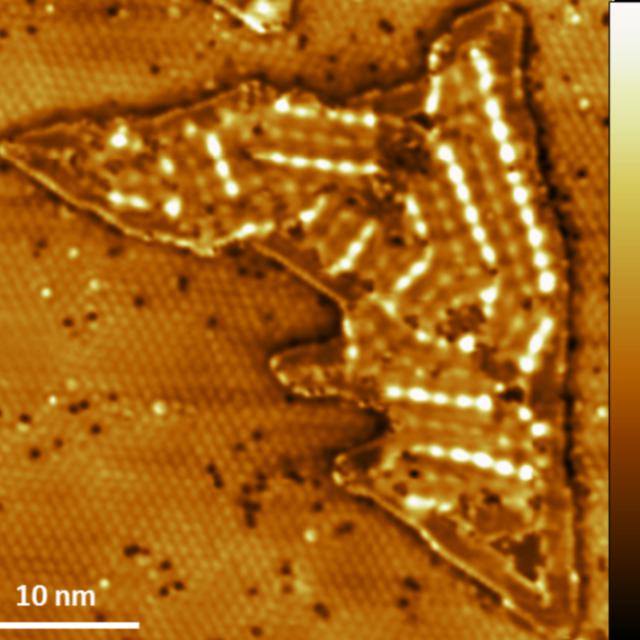 Spin-polarized STM image of the hexagonal nanoskyrmion lattice in a Fe monolayer and the spin spiral in the iron bilayer on Ir(111). (T = 6 K)